
Xilinx, Inc. , the leader in adaptive and intelligent computing, today announced the expansion of its 16 nanometer (nm) Virtex® UltraScale+™ family to now include the world’s largest FPGA — the Virtex UltraScale+ VU19P. With 35 billion transistors, the VU19P provides the highest logic density and I/O count on a single device ever built, enabling emulation and prototyping of tomorrow’s most advanced ASIC and SoC technologies, as well as test, measurement, compute, networking, aerospace and defense-related applications.
The VU19P sets a new standard in FPGAs, featuring 9 million system logic cells, up to 1.5 terabits per-second of DDR4 memory bandwidth and up to 4.5 terabits per-second of transceiver bandwidth, and over 2,000 user I/Os. It enables the prototyping and emulation of today’s most complex SoCs as well as the development of emerging, complex algorithms such as those used for artificial intelligence, machine learning, video processing and sensor fusion. The VU19P is 1.6X larger than its predecessor and what was previously the industry’s largest FPGA — the 20 nm Virtex UltraScale 440 FPGA.
“The VU19P enables developers to accelerate hardware validation and begin software integration before their ASIC or SoC is available,” said Sumit Shah, senior director, product line marketing and management, Xilinx. “This is our third generation of world-record FPGAs. First was the Virtex-7 2000T, followed by the Virtex UltraScale VU440, and now the Virtex UltraScale+ VU19P. But this is more than silicon technology; we’re providing robust and proven tool flows and IP to support it.”
The VU19P is supported by an extensive set of debug, visibility tools, and IP, providing customers with a comprehensive development platform to quickly design and validate next-generation applications and technologies. Hardware and software co-validation allows for developers to bring up software and implement custom features before physical parts are available. Moreover, the design flow can be co-optimized by using the Xilinx Vivado® Design Suite, which reduces cost and tape-out risk, and improves efficiency and time-to-market.
“Arm relies on Xilinx devices as part of our process for validating our next-generation processor IP and SoC technology,” said Tran Nguyen, director of design services, Arm. “The new VU19P will further enable Arm, and many others in our ecosystem, to accelerate the design, development and validation of our most ambitious roadmap technologies.”
All registered trademarks and other trademarks belong to their respective owners. For more details, please visit Xilinx official site.
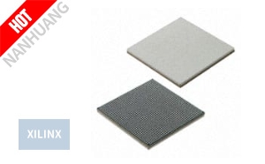 IC FPGA 850 I/O 1761FCBGA
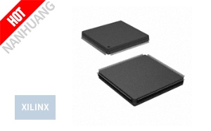 IC FPGA 140 I/O 208QFP
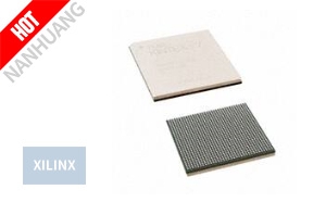 IC FPGA 600 I/O 1156FCBGA
 IC FPGA 360 I/O 665FCBGA
 IC CPLD 108MC 7.5NS 100TQFP
 IC FPGA 400 I/O 676FCBGA
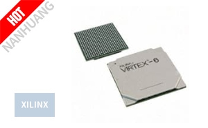 IC FPGA 720 I/O 1759FCBGA
 IC FPGA 108 I/O 144TQFP
 IC CPLD 72MC 15NS 44PLCC
 IC FPGA 360 I/O 665FCBGA
 IC FPGA 320 I/O 484CSBGA
 IC FPGA 360 I/O 665FCBGA


- Avnet introduces Kintex UltraScale all programmable FPGA development kit
- Users can reuse their Xilinx1153 ICs with easy to use BGA adapter set
- 25G/50G low-latency Ethernet MAC, optimized for Xilinx Ultrascale+ transceiver technology
- Optical interconnect demos PCIe links over FPGA board
- PRO DESIGN expands prototyping portfolio with ultra-fast proFPGA Virtex® UltraScale+™ based FPGA mo
- Z-turn Board – Xilinx ZYNQ-7010/20 SoC based ARM Cortex-A9 single board compute
- Xilinx Artix UltraScale+ FPGA development platform released
- Xilinx unveils industry’s largest FPGA
- AMD rolls out 5G RF chips and test services
- FPGA development module released for Xilinx Artix UltraScale+
- Why test must follow design’s example by adopting a platform-based approach
- 2-GHz oscilloscope adds jitter and real-time eye analysis packages
